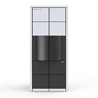
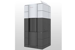
A perfect combination of the best image resolution and the highest analytical efficiency
The Themis S TEM is an 80-200 kV scanning/transmission electron microscope (S/TEM) designed for
high-speed imaging and analysis of semiconductor devices.
| Specifications | ||
|---|---|---|
| High tension range | 80-200 keV | |
| Electron source | X-FEG | |
| TEM information limit | 0.11 nm | |
| Probe corrector option | No | Yes |
| STEM resolution at 200kV (nm) | 0.164 | 0.083 |
| STEM resolution at 80kV (nm) | 0.31 | 0.136 |
| EDS collection angle (shadowing removed) | 1.8 srd | |
| OptiSTEM | Included | |
| iDPC | Optional | |
| STEM detectors | HAADF/BF/DF2/DF4 | |
| Camera | Ceta 4k × 4k CMOS | |

